Digital logic and EDA tutorials
Verilog models, testbenches, FPGA experiments, and tutorials covering circuit simulation and physical verification.
14 matching resources
- Project Digital logic and EDA tutorialsProject period 2012–2014
- Published
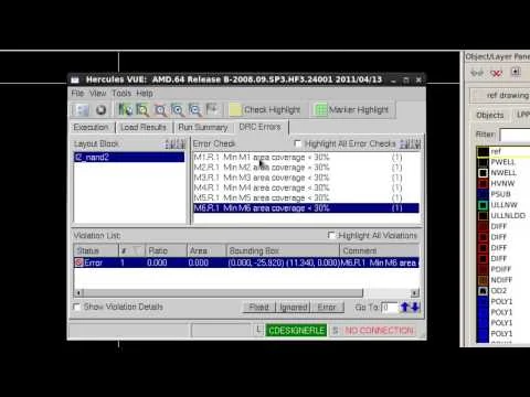
An introduction to HSpice, physical verification, parasitic extraction, and schematic-to-layout comparison through a NAND example.
- Published
A practical continuation of the Synopsys tool flow, focused on entering and simulating a circuit.
- Video Synopsys VCS on CentOSPublished
A recorded walkthrough of the Verilog simulation environment using VCS on Linux.
- Video CMOS JK flip-flopPublished
A circuit-level study of a JK flip-flop, part of the digital-design teaching archive.
- Video CMOS D-latchPublished
A CMOS latch example connecting transistor-level implementation with digital behavior.
- Published
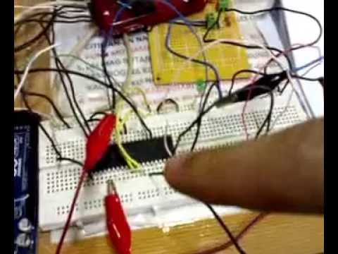
A board-based FPGA experiment from the hardware and digital-logic archive.
- Published
An experiment in the timing logic needed to generate a VGA display signal.
- Published
A small counter design used to explore the Xilinx development workflow.
- Published
A counter example connecting HDL development with simulation in the Altera toolchain.
- Published
A short visual record of counter behavior; useful alongside the narrated HDL examples.
- Published
A demonstration of arithmetic logic from the collection of small Verilog designs.
- Published
An introductory recording of the development workflow around a Verilog design.
- Published
An introduction to working with Verilog using freely available simulation tooling.